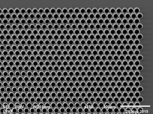
Laser-Induced Deep Etching (LIDE)
High-aspect ratio microfeatures in glass
What is LIDE?
LIDE stands for laser induced deep etching
LIDE technology is a two-step process. It is characterized by the ability to create deep structures in thin glass with a high aspect ratio in the range of >1:10 at a highly-economical processing speed not seen before. Structures as small as <5 μm can be created.
Step 1:
In the first step, the glass is locally modified by laser pulses according to the desired layout. In LIDE, a single laser pulse is sufficient to modify glass substrates through their entire thickness, making it compatible with high-volume production.
Step 2:
In the second process step, the modified areas of the glass are removed by wet chemical etching much more rapidly than the unmodified material is.
Outstanding characteristics of LIDE technology
LIDE technology is free of micro-cracks, chipping, induced stresses and the like. LIDE processing of glasses does not diminish the good mechanical properties of glass as it can be found in state-of-the art glass-processing technologies.
LIDE does not rely on special glasses. The technology is compatible with all commercially-available silicate-based glass types from different vendors.
Why glass?
A low-cost material with a unique set of properties
Glass is of great interest as a material for a variety of applications in micro systems technology due to its unique set of properties. Thin glass is available in various formats such as wafer- and panel-size formats.
General properties driving glass applications:
- Optical
- High transparency
- Low fluorescence
- Chemical and mechanical
- High chemical resistance and chemically inert
- Isotropic
- Good mechanical stability
- Low thermal expansion
- Tunable coefficient of thermal expansion
- Electrical
- Perfect isolator
- Low insertion loss
- Smooth surface enabling fine-line lithography


