Glass Embedding Wafer
Next Level Advanced Packaging
- Limited die shift especially
- Passive die alignment for lowest die position inaccuracies
- Lower warpage due to high Young's modulus of glass
- Can be combined with Through Glass Vias and Integrated Passives
- Can readily be scaled to panel-level-manufacturing

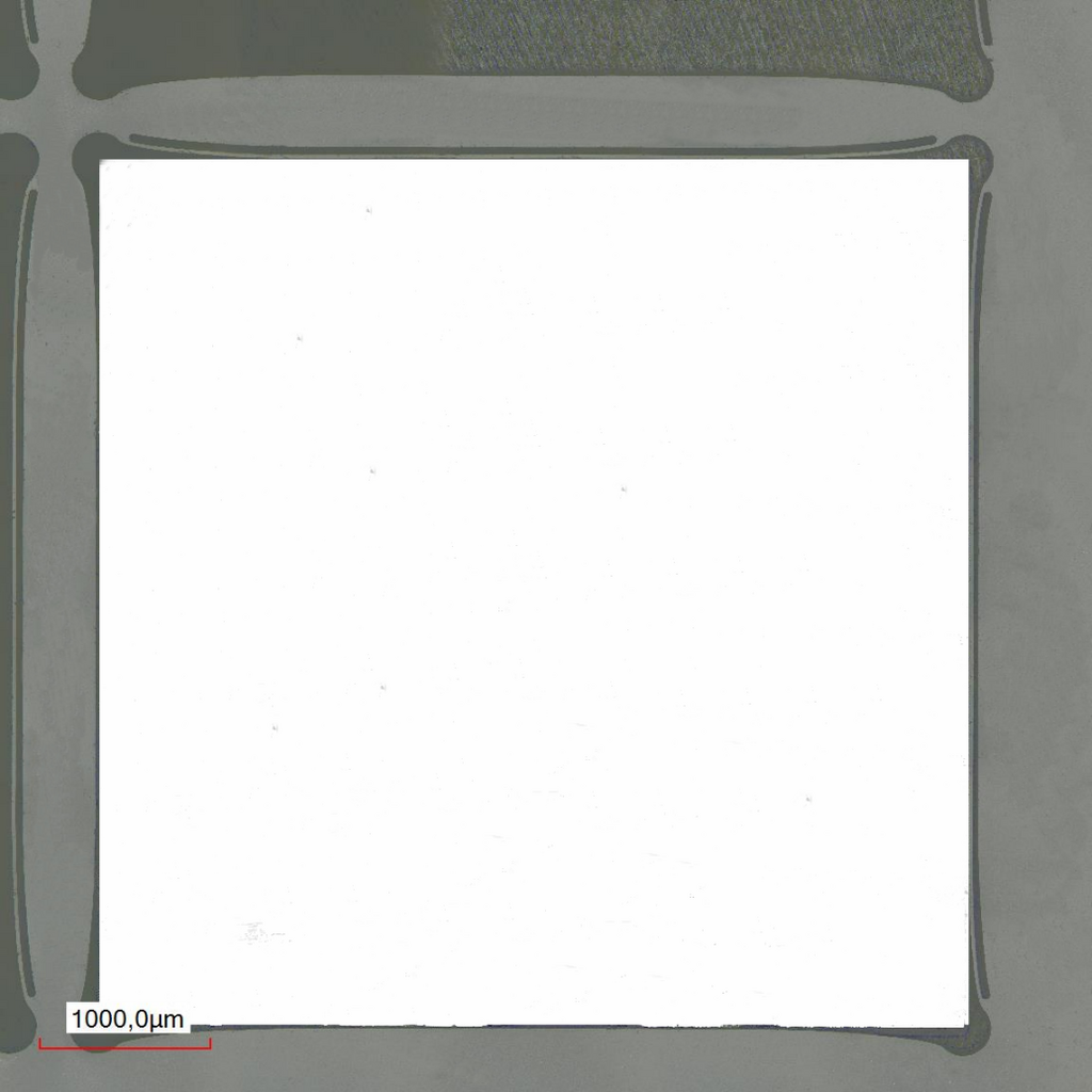
Glass Wafer
- Glass Thickness: <0.9 mm
- Minimum aperture: 10 µm (round)
- Positional accuracy: +-5 µm
- Taper Angle: 1° to 7° (depending on glass type)
- Chipping: None
- Microcracks: None
- Substrate Size and Format: All standard wafer sizes up to 450 mm and glass panels up to 510x510 mm²
Download
Glass Embedding Wafer (PDF - 212,36 KB)
Pricing
LIDE is a high throughput technology which allows us to offer high quality glass substrates at an appealing price point. Let us convince you.